Home
/ Fermi Level Definition In Semiconductors / Fermi Level In Extrinsic Semiconductor / It is a thermodynamic quantity usually denoted by µ or e f for brevity.
Fermi Level Definition In Semiconductors / Fermi Level In Extrinsic Semiconductor / It is a thermodynamic quantity usually denoted by µ or e f for brevity.
Fermi Level Definition In Semiconductors / Fermi Level In Extrinsic Semiconductor / It is a thermodynamic quantity usually denoted by µ or e f for brevity.. Smith department of eecs university of california, berkeley eecs 105 spring 2004, lecture 19 prof. For solid materials such as metals, the orbital occupancy can be calculated by making an approximation based on the crystalline structure. Fermi level is a reference level which is just above all the electron energy level. The fermi level is a hypothetical level of potential energy for an electron inside a crystalline solid. The position of the fermi level for the conduction band is a vital parameter in determining the electrical properties.
The fermi level does not include the work required to remove the electron from wherever it came from. The level of occupancy determines the conductivity of different materials. Fermi level the fermi level is the energy level which is occupied by the electron orbital at temperature equals 0 k. The fermi level is at e / u = 1 and k t = u. The fermi level is the surface of fermi sea at absolute zero where no electrons will have enough energy to rise above the surface.
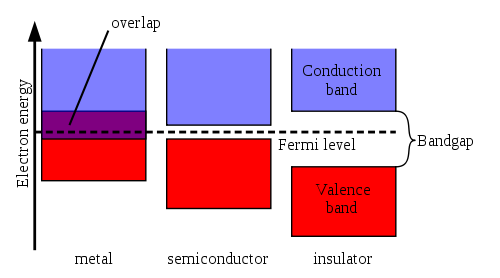
Conduction Band Energy Education from energyeducation.ca A precise understanding of the fermi level—how it relates to electronic band structure in determining electronic. A semiconductor is a solid that is defined as having its fermi level (chemical potential) in a band gap of the electronic structure of the solid, which is not too large compared to the thermal energy, so that, according to the fermi distribution, at room temperature you have a significant number of electrons and/or holes in the conduction and valence band available for conduction. Very small energy required by an electron to reach this level from valance band. While at t = 0 k the fermi function equals a step function, the transition is more gradual at finite temperatures and more so at higher. The fermi level is a hypothetical level of potential energy for an electron inside a crystalline solid. Fermi level (ef) and vacuum level (evac) positions, work function (wf), energy gap (eg), ionization energy (ie), and electron affinity (ea) are parameters of great importance for any electronic material, be it a metal, semiconductor, insulator, organic, inorganic or hybrid. Fermi level is a kind of measure of equilibrium electronic energy of a solid material. N d is the concentration of donar atoms.
Fermi level is a reference level which is just above all the electron energy level.
In practice, the fermi level is usually calculated with respect to conduction band bottom or top of the valence band and for a homogenous semiconductor. (at zero degree kelvin) it means that no electron is present above this level. The fermi level is at e / u = 1 and k t = u. For solid materials such as metals, the orbital occupancy can be calculated by making an approximation based on the crystalline structure. Smith context the first part of this lecture is a review of electrons and holes in silicon: Fermi level the fermi level is the energy level which is occupied by the electron orbital at temperature equals 0 k. In metals, the fermi energy gives us information about the velocities of the electrons which participate in ordinary electrical conduction. However as the temperature increases free electrons and holes gets generated. In the semiconductor, free charge carriers are electrons and electron holes (electron The fermi level lies between the valence band and conduction band because at absolute zero temperature the electrons are all in the lowest energy state. Whenever the system is at the fermi level, the population n is equal to 1/2. Fermi level is an important part of this theory which states about the top of the available electron energy levels at low temperatures. At absolute zero temperature intrinsic semiconductor acts as perfect insulator.
E c is the conduction band. Very small energy required by an electron to reach this level from valance band. Fermi level the fermi level is the energy level which is occupied by the electron orbital at temperature equals 0 k. The level of occupancy determines the conductivity of different materials. Fermi level is an important part of this theory which states about the top of the available electron energy levels at low temperatures.
Quasi Fermi Levels Explained Youtube from i.ytimg.com The fermi level does not include the work required to remove the electron from wherever it came from. In practice, the fermi level is usually calculated with respect to conduction band bottom or top of the valence band and for a homogenous semiconductor. The fermi function has a value of one for energies, which are more than a few times kt below the fermi energy. Fermi levels, forward bias prof j. In thermal equilibrium the probability of finding an energy level at e occupied is given by the fermi function, f(e): The fermi level is the energy level which is occupied by the electron orbital at temperature equals 0 k. The number of free electron depend on the impurity atom added. Smith context the first part of this lecture is a review of electrons and holes in silicon:
If you can bring the fermi level high enough, then part of the tail will go over to the conduction band.
A precise understanding of the fermi level—how it relates to electronic band structure in determining electronic. At absolute zero temperature intrinsic semiconductor acts as perfect insulator. In semiconductors the position of the fermi level is within the band gap, approximately in the middle of the band gap. 3 m * for intrinsic semiconductor we previously found: In metals, the fermi level lies in the hypothetical conduction band giving rise to free conduction electrons. Smith department of eecs university of california, berkeley eecs 105 spring 2004, lecture 19 prof. (at zero degree kelvin) it means that no electron is present above this level. The level of occupancy determines the conductivity of different materials. In the semiconductor, free charge carriers are electrons and electron holes (electron Fermi level (ef) and vacuum level (evac) positions, work function (wf), energy gap (eg), ionization energy (ie), and electron affinity (ea) are parameters of great importance for any electronic material, be it a metal, semiconductor, insulator, organic, inorganic or hybrid. Let ed and nd be the energy and number of electron of the donor. A semiconductor is a solid that is defined as having its fermi level (chemical potential) in a band gap of the electronic structure of the solid, which is not too large compared to the thermal energy, so that, according to the fermi distribution, at room temperature you have a significant number of electrons and/or holes in the conduction and valence band available for conduction. Fermi level is a kind of measure of equilibrium electronic energy of a solid material.
N d is the concentration of donar atoms. In semiconductors the position of the fermi level is within the band gap, approximately in the middle of the band gap. However as the temperature increases free electrons and holes gets generated. Due to this, a hole is created in the adjacent atom. The fermi function has a value of one for energies, which are more than a few times kt below the fermi energy.
Limitation Of Fermi Level Shifts By Polaron Defect States In Hematite Photoelectrodes Nature Communications from media.springernature.com The fermi level is referred to as the electron chemical potential in other contexts. It usually depends on the material and the concentration of impurities. For solid materials such as metals, the orbital occupancy can be calculated by making an approximation based on the crystalline structure. The fermi level does not include the work required to remove the electron from wherever it came from. The fermi level lies between the valence band and conduction band because at absolute zero temperature the electrons are all in the lowest energy state. Whenever the system is at the fermi level, the population n is equal to 1/2. N d is the concentration of donar atoms. Fermi levels, forward bias prof j.
The fermi level is the energy level which is occupied by the electron orbital at temperature equals 0 k.
If you can bring the fermi level high enough, then part of the tail will go over to the conduction band. In pure semiconductors the position of the fermi level is within the band gap, approximately. The fermi level is referred to as the electron chemical potential in other contexts. In metals, the fermi level lies in the hypothetical conduction band giving rise to free conduction electrons. Smith department of eecs university of california, berkeley eecs 105 spring 2004, lecture 19 prof. Position of fermi level in extrinsic semiconductors • here the situation is different due to impurity of trivalent and pentavalent. K b is the boltzmann constant. (at zero degree kelvin) it means that no electron is present above this level. The fermi level does not include the work required to remove the electron from wherever it came from. Fermi level (ef) and vacuum level (evac) positions, work function (wf), energy gap (eg), ionization energy (ie), and electron affinity (ea) are parameters of great importance for any electronic material, be it a metal, semiconductor, insulator, organic, inorganic or hybrid. The level of occupancy determines the conductivity of different materials. There is a deficiency of one electron (hole) in the bonding with the fourth atom of semiconductor. A semiconductor is a solid that is defined as having its fermi level (chemical potential) in a band gap of the electronic structure of the solid, which is not too large compared to the thermal energy, so that, according to the fermi distribution, at room temperature you have a significant number of electrons and/or holes in the conduction and valence band available for conduction.
In the semiconductor, free charge carriers are electrons and electron holes (electron fermi level in semiconductor. E c is the conduction band.